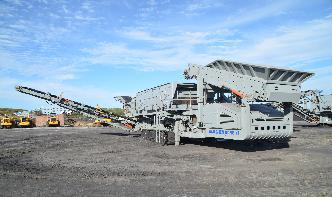
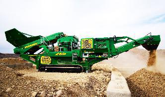
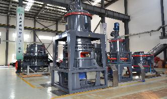
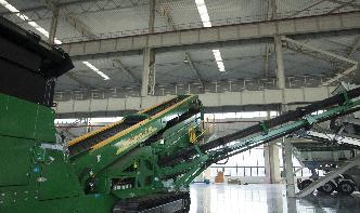
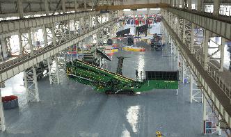
مصنع لتجهيز البوكسيت/Silica Grinding Area Process Flow Diagram
process flow diagrams for the Bayer process and the HallHeroult process. 2. Generalized Process Fl ow Diagram Bayer Process A process flow diagram of the Bayer process is shown in Exhibit 3. The primary purpose of a Bayer plant is to process bauxite to provide pure alumina for the production of aluminum. All bauxite refineries share five common
increment of surface area 24 . Synthesis of silica aerogel and silica xerogel 28 Flow diagram of drug loading procedure via impregnation and physical mixing methods 32 Flow diagram of drug loading procedure via direct synthesis method 33 Schematic diagram of supercritical carbon dioxide 34 Typical BET plot 40
Convert the following flow chart into a paragraph of about 150 words. The process of making cement is described in this flow chart. The two raw materials used in theprocess are limestone and clay. Limestone is crushed, sized, dried and stored in storage silos. In the same way, Clay is washed, crushed, and dried in storage basins. The two materials are mixed in the correct proportion and ground ...
per unit area 34 area Energy input ' T K 2 d t K K b l u b l d T K u ' 1 2 2 1 D d Vcr v T K K d 4 1 ' 1 2 ME 338: Manufacturing Processes II Instructor: Ramesh Singh; Notes: Profs. Singh/Melkote/Colton Grinding temperature • Rearranging ∆𝑇=𝐾1𝐾2 3 4 𝑉 𝑟 4 𝑣 𝐷 • Temperatures can be up to 1600oC, but for a short time. 35. ME 338: Manufacturing Processes II Instructor ...
Wafer backgrinding is a semiconductor device fabriion step during which wafer thickness is reduced to allow stacking and highdensity packaging of integrated circuits (IC).. ICs are produced on semiconductor wafers that undergo a multitude of processing steps. The silicon wafers predominantly used today have diameters of 200 and 300 mm. They are roughly 750 μm thick to ensure a minimum .
processes replaced almost completely the aluminium oxide processes (1893) and the green silicon carbide processes (1891). Other nonconventional processes include powder metallurgy processes used to produce hardalloy cutting tools made of tungsten carbide, titanium carbide, cobalt carbide, etc.
silicon chip. The second, assembly, is the highly precise and automated process of packaging the die. Those two phases are commonly known as " FrontEnd " and " BackEnd ". They include two test steps: wafer probing and final test. Figure 1. Manufacturing Flow Chart of an Integrated Circuit WAFER FABRICATION (FRONTEND)
silicon dioxide oxygen chlorine silicon tetrachloride Prior art date Legal status (The legal status is an assumption and is not a legal conclusion. Google has not performed a legal analysis and makes no representation as to the accuracy of the status listed.) Expired Lifetime Appliion number US739418A Inventor Hughes William Evans Arthur Wallace Current Assignee (The listed ...
Figure presents a general process flow diagram for ceramic products manufacturing. The basic steps include raw material procurement, beneficiation, mixing, forming, green machining, drying, presinter thermal processing, glazing, firing, final processing, and packaging. The following paragraphs describe these operations in detail. Raw Material Procurement To begin the process ...
Simplified or conceptual designs are called process flow diagrams (PFDs). A PFD shows fewer details than a PID and is usually the first step in the design process–more of a 's eye view. More fully developed piping and instrumentation diagrams (PIDs) are shown in a PID. What are the limitations of PID? Since PIDs are graphic representations of processes, they have some inherent ...
granulation plant. The flow diagram is based on the addition of UF85 liquid urea/formaldehyde precondensate. The process flow diagram of Granular Urea Plant is shown in Figure above. 295. The used ambient air contains entrained urea dust and the traces of ammonia which is washed in the granulator dust scrubber.
· Back End(BE) Process Wafer Back Grinding • The typical wafer supplied from 'wafer fab' is 600 to 750μm thick. • Wafer thinned down to the required thickness, 50um to 75um, by abrasive grinding wheel. › 1st step : Use a large grit to coarsely grind the wafer and remove the bulk of the excess wafer thickness. › 2nd step : Use a finer grit to polish the wafer and to accurately grind ...
silica grinding area process flow diagram . Improving performance of milled powder with AEROSIL fumed Jan 25, 2017 grinding process or mixed in a step before. The surface of the finely milled . Get Price silica sand mining process flow chart devalklier. Posts Related to sand wash plant flow diagram. Silica Sand Mining Process silica production flow chart,silica grinding area process flow ...
silica grinding area process flow diagram. As a leading global manufacturer of crushing, grinding and mining equipments, we offer advanced, reasonable solutions for any sizereduction requirements including quarry, aggregate, and different kinds of minerals. We can provide you the complete stone crushing and beneficiation also supply standalone crushers, mills and beneficiation ...
CMOS Process at a Glance Define active areas Etch and fill trenches Implant well regions Deposit and pattern polysilicon layer Implant source and drain regions and substrate contacts Create contact and via windows Deposit and pattern metal layers. Digital Integrated Circuits Manufacturing Process EE141 CMOS Process WalkThrough p+ pepi (a) Base material: p+ substrate with pepilayer p+ (c ...
Process flow diagrams (PFDs) are used in chemical and process engineering. These diagrams show the flow of chemicals and the equipment involved in the process. Generally, a Process Flow Diagram shows only the major equipment and doesn't show details. PFDs are used for visitor information and new employee training. A Process and Instrument Drawing (PID) includes more details than a PFD. It ...
experimental box diagram and apparatus are shown in Figs. 1 and 2, respectively. Characterization The formed products were characterized by particle size distribution, zeta potential (Malvern Zeta Sizer 3000 HSA), TEM(Philips, CM 200FEG) and accelerated Fig. 1: .
· grinding process. As the polishing process continues, the pitch will slowly conform to the shape of the optic so that the surface of the optic is smoothed out, but its overall radius is not changed. To aid in removing debris, grooves are cut along the pitch to allow slurry to flow more readily between the tool and the optic. A hole is also cut in the pitch at the center of the tool since pitch ...
• Kovacs, "Bulk Micromachining of Silicon," pp. 153643. • Williams, "Etch Rates for Micromachining Processing," pp. 25660. • Senturia, Chapter 3, "Microfabriion." • Today's Lecture • Tools Needed for MEMS Fabriion • Photolithography Review • Crystal Structure of Silicon • Bulk Silicon .
volume of air 1metre above the area of a football (soccer) field Teaspoon 1 metre high X 1 X 50 Concentrations are expressed as milligrams per cubic metre (mg/m³) for solids or parts per million (ppm) for gases. It is not always easy to picture what 1mg/m³ or 1ppm actually means, so the diagrams below may help to get some idea of the scale.
A STUDY ON ULTRA FINE GRINDING OF SILICA AND TALC . IN OPPOSED FLUIDIZED BED JET MILL . by . ... Parameters affecting fine grinding process in jet mill . 19 . iii. ... Schematic diagram of grinding and classifying chamber of jet mill . 68 . Figure (a) Nozzles in .